


What are the component packages?
2022-10-10 17:23
In smt贴片加工In the production of the factory, we can often see all kinds of components, especially the components on some boards during smt proofing and mounting. Now Jingbang will show you the basic structure of various components.
1. Component packaging
Package refers to the layout and structure of component pins. It is the object of assembly and the basis of design for manufacturability of PCBA.
2. Packaging form of surface mounted components
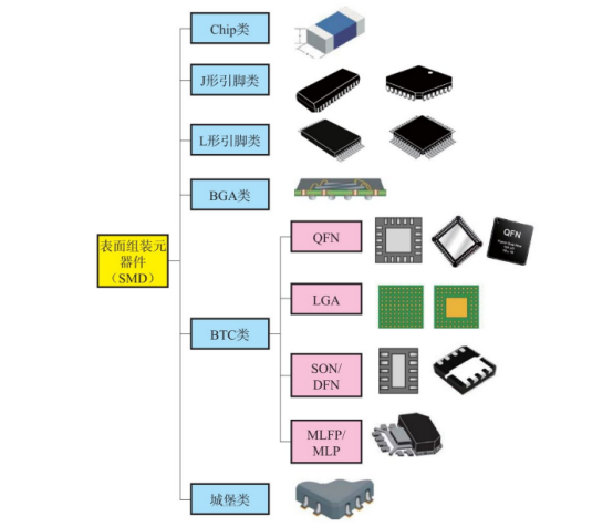
SMT professional SMT chip processing component layout, pad design, solder mask design and stencil design all take the encapsulated pin structure form as the object. Therefore, we do not classify SMT processing by the package name but by the pin or solder end structure form. According to this classification, surface mount device (SMD) packaging mainly includes Chip, J-shaped pin, L-shaped pin, BGA, BTC and castle, as shown in the figure below
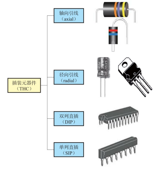
The packaging form of the plug-in components in the chip production. If the THC packaging is classified according to the structure type of the lead, there are four major categories, namely, axial lead, radial lead, single in line and dual in line (DIP), as shown in Figure
3. Description of abbreviations
(1) BGA, the abbreviation of Ball Grid Array, can be translated into ball grid array package. Its welding end is a solder ball and is arranged at the bottom of the package in the form of an array. The ball Grid array package includes the full array and the peripheral Array. The standard Ball center distances are 1. 50mm, 1. 00mm, 0. 80mm, 0. 65mm, 0. 50mm, 0. 40mm and 0. 35mm.
(2) BTC, the abbreviation of Bottom Termination Component, can be translated as bottom face end package. Its welding end is flat and arranged on the bottom of the package. BTC packaging includes QFN, LGA, SON, DFN, MLFP, MLP and other packaging forms.
(3) QFN, the abbreviation of Quad Flat No Lead Package, can be translated into square flat no pin package, with flat welding ends arranged on four sides of the package bottom.
(4) LGA, the abbreviation of Land Grid Array, can be translated as a pad grid array package. Its solder ends are planar and arranged at the bottom of the package in the form of an array.
(5) SON, the abbreviation of Small Outline No Lead, can be translated as a small footprint no pin package, with its welding ends being flat and arranged on both sides of the package bottom.
(6) MLP, the abbreviation of Micro Leadframe Package, can be translated as micro lead frame package. Its welding ends are flat and arranged on the four sides of the package bottom, which can be understood as small QFN.
Related Articles

2022-10-08
2022-10-08
Follow us
